Get a Sample
Request engineering samples to evaluate fit, validate alternatives, and keep design decisions moving before a larger order is placed.
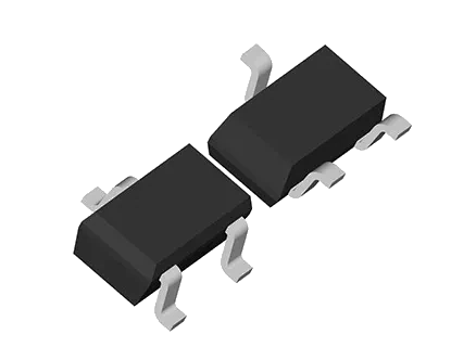
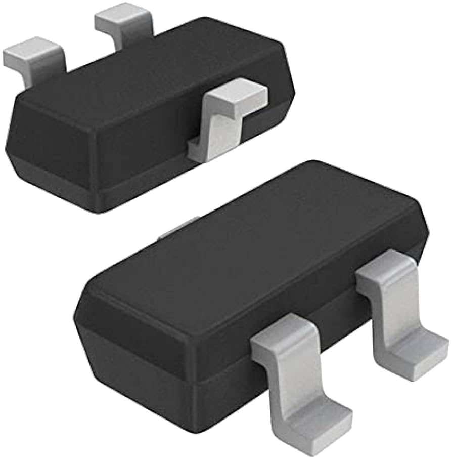
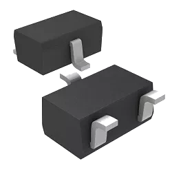
Request evaluation samplesFDN5618P is a Transistors - FETs, MOSFETs - Single model from ON Semiconductor, presented on TrustCompo for buyers who need clear sourcing and review context before RFQ. This listing sits in the Discrete Semiconductor Products / Transistors - FETs, MOSFETs - Single product path. Known package information currently points to SSOT3 under the ON Semiconductor brand listing. MOSFET P-CH 60V 1.25A SSOT3. TrustCompo combines the available model, brand, hierarchy, and specification details around FDN5618P so buyers can move faster from review to quotation.
Traceability and authenticity checks
Fast RFQ turnaround
Documentation support
Pre-shipment inspection review
Key specifications
Series
PowerTrench®
Min Quantity
1
Category
Discrete Semiconductor ProductsSub Category
Transistors - FETs, MOSFETs - SingleDescription
MOSFET P-CH 60V 1.25A SSOT3
key Attributes
-
Datasheet
View FDN5618P DatasheetTechnical document
Review the latest datasheet for FDN5618P from ON Semiconductor in a separate tab so engineers and buyers can check package, electrical characteristics, and application details without leaving this product page.
Why request a quote
Use the RFQ step to confirm the commercial and documentation details buyers usually need before placing an order.
Trust signals
Globally recognized certifications
Visible certifications work best when they are paired with clear operational promises around traceability, handling, and inspection.
ISO 9001
Quality management processes for more consistent sourcing and handling.
AS9120B
Aerospace-focused distribution controls for traceability and reliability.
ISO 14001
Environmental management discipline across warehouse and operating workflows.
ESD Control
Electrostatic handling standards to help protect sensitive components.
Ordering workflow
Use this section to see the fastest ordering path and the policy pages buyers usually review before confirming a component order.
How to order this product
A simple B2B flow helps engineering and procurement teams move from part review to commercial confirmation.
Review the part number, package, key specs, and target quantity so the quote request reflects the exact sourcing scope your team needs.
Use Quick Quote for commercial pricing or Request Sample when engineering validation is still in progress and a smaller evaluation quantity is needed.
Before final release, confirm stock timing, shipment method, payment arrangement, and any traceability or inspection documents required by your process.
Policies buyers usually check
These pages explain the operating rules around samples, shipping, payment, and quality support before you place the order.
Request engineering samples to evaluate fit, validate alternatives, and keep design decisions moving before a larger order is placed.
Request evaluation samplesReview shipping origin, carrier options, delivery methods, and the practical factors that affect transit timing for global component orders.
Review shipping detailsUnderstand supported payment methods, invoice handling, quote currency, and the commercial boundaries used for international B2B orders.
Review payment termsSee how incoming inspection, outgoing verification, traceability support, certifications, and additional testing fit into our quality workflow.
Review quality controlsStructured product content
Review overview, detailed specifications, and related sourcing content in one structured flow without scanning separate oversized sections.
Product overview
The FDN5618P is a dual N-channel MOSFET (Metal-Oxide-Semiconductor Field-Effect Transistor) manufactured by ON Semiconductor. It is designed for various applications, including power management, switching, and signal amplification. Here’s a detailed description of its features and specifications:
The FDN5618P is suitable for a variety of applications, including:
In summary, the FDN5618P from ON Semiconductor is a versatile and efficient dual N-channel MOSFET that offers low on-resistance, high current handling, and fast switching capabilities. Its compact SOT-23 package and robust electrical characteristics make it an excellent choice for a wide range of electronic applications, particularly in power management and control systems.
Fast scan
Export Classifications & Environmental
JESD-609 Code
e3
Export Classifications & Environmental
Moisture Sensitivity Level (MSL)
1 (Unlimited)
Export Classifications & Environmental
ECCN Code
EAR99
Export Classifications & Environmental
RoHS Status
ROHS3 Compliant
Export Classifications & Environmental
REACH SVHC
No SVHC
Export Classifications & Environmental
HTSUS
8541.21.0095
Common questions
Quick answers for buyers reviewing FDN5618P, stock, documentation, and sourcing steps.
FDN5618P is a Transistors - FETs, MOSFETs - Single component from ON Semiconductor. This product page summarizes the core sourcing details buyers need before checking price, availability, documentation, or samples.
FDN5618P is listed with package reference SSOT3. The current product description is MOSFET P-CH 60V 1.25A SSOT3, and buyers should confirm package, footprint, and electrical details against the datasheet or quotation notes before approval.
This page currently shows 55201 units in stock and 43198 units available for FDN5618P. Because electronic component availability can change quickly, submit an RFQ to confirm live stock, lead time, and final pricing.
Yes. Use the Quick Quote or Request Sample action on this page to send the quantity and sourcing requirements for FDN5618P by ON Semiconductor. The TrustCompo team can review price, availability, and documentation support.
Yes. This page links to the datasheet for FDN5618P by ON Semiconductor, so engineers and buyers can review package, ratings, and application details before purchase.
Buyers should confirm the manufacturer, package, quantity, target price, RoHS or compliance needs, and any Certificate of Conformance or traceability requirements for FDN5618P before approving the order.
Transistors - FETs, MOSFETs - Single
Explore more parts from the same subcategory to compare fit, stock, and sourcing options.
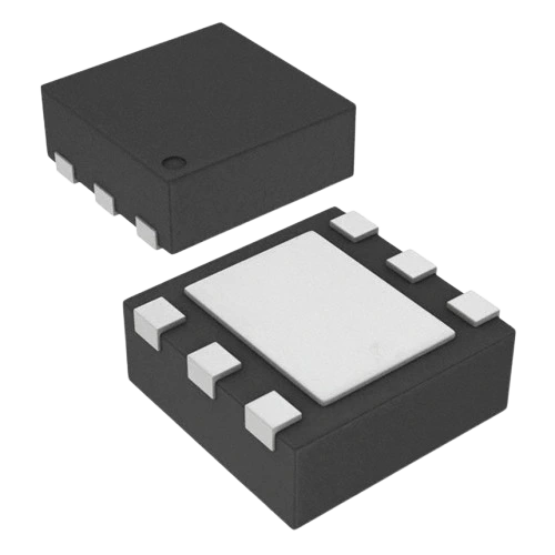


MOSFET P-CH 20V 12A SC70-6

More sourcing insights
Explore related articles around FDN5618P, Transistors - FETs, MOSFETs - Single, and adjacent sourcing decisions so buyers can compare context before moving from evaluation to RFQ.
Jul 17, 2026
FPGA Supply 2026: A Buyer's Framework for AMD Xilinx, Intel Altera, Microchip, and Lattice SourcingA production-BOM FPGA sourcing guide for 2026 covering lifecycle commitment, redesign cost, and qualification boundaries across AMD Xilinx, Intel Altera, Microchip PolarFire, and Lattice families.
Jul 11, 2026
2026 Q3 Wide-Bandgap Power Read: Where SiC Is Scaling, Where GaN Is Winning, and Why Silicon Still MattersA Q3 2026 read on SiC, GaN, and silicon power semiconductors: where wide-bandgap devices are winning now, where silicon still holds, and what engineers and sourcing teams should watch.
Jul 8, 2026
Texas Instruments Lead Time and Price Pressure in 2026: What Analog and Power Buyers Should Do NowA buyer-facing framework for Texas Instruments analog and power IC exposure in 2026, covering what is confirmed, where price and lead-time pressure is most likely to show up, and which actions sourcing teams should take first.