
MRAM in Aerospace Applications: Where Radiation Tolerance Actually Matters for Mission Memory
A buyer-facing MRAM aerospace guide covering where magnetic memory earns its premium, what radiation tolerance does and does not solve, and why Everspin-class discrete MRAM still matters in mission-oriented electronics planning.
Quick facts
- MRAM is attractive in aerospace because it combines non-volatility, fast writes, and high endurance without flash-style erase management.
- The strongest aerospace fit is usually boot, configuration, event logging, and fast-recovery memory, not bulk payload storage.
- Radiation resilience is a real advantage, but the MRAM cell is only part of the story; peripheral CMOS, package, and board-level design still set the real qualification boundary.
- For procurement teams, the practical questions are application fit, qualification evidence, lifecycle stability, and whether discrete MRAM supply is available from established vendors such as Everspin.
Many MRAM articles start with the physics and end with a broad claim that "space needs radiation-hard memory." That framing is incomplete. Aerospace programs do not buy memory because a technology sounds advanced. They buy it because a specific memory role has a failure cost, a recovery-time requirement, and a qualification burden that other memory types handle poorly.
This article is written for that decision point. It is not a generic introduction to MRAM and it is not a flight-qualification certificate. It is a buyer-facing and engineer-facing framework for deciding where MRAM earns its premium in aerospace systems, where it does not, and why discrete suppliers such as Everspin continue to matter.
1. The real aerospace question is not "Is MRAM space-grade?"
TC judgment The better question is: which memory jobs become simpler, safer, or easier to recover when the design uses MRAM instead of SRAM, DRAM, EEPROM, or NOR flash?
That distinction matters because aerospace memory roles are not all the same:
| Memory role | What the system needs most | Why MRAM may help |
|---|---|---|
| Boot and configuration storage | Data must survive power loss and be available immediately after reset | MRAM is non-volatile and does not need flash erase housekeeping |
| Fault and event logging | Repeated writes with high confidence during abnormal events | MRAM handles frequent writes better than flash-style endurance-limited memory |
| Persistent working data | Fast save-and-recover behavior | MRAM can shorten recovery logic and reduce firmware complexity |
| Bulk payload storage | Low cost per bit and high density | MRAM is usually weaker here because density and cost are not its main strengths |
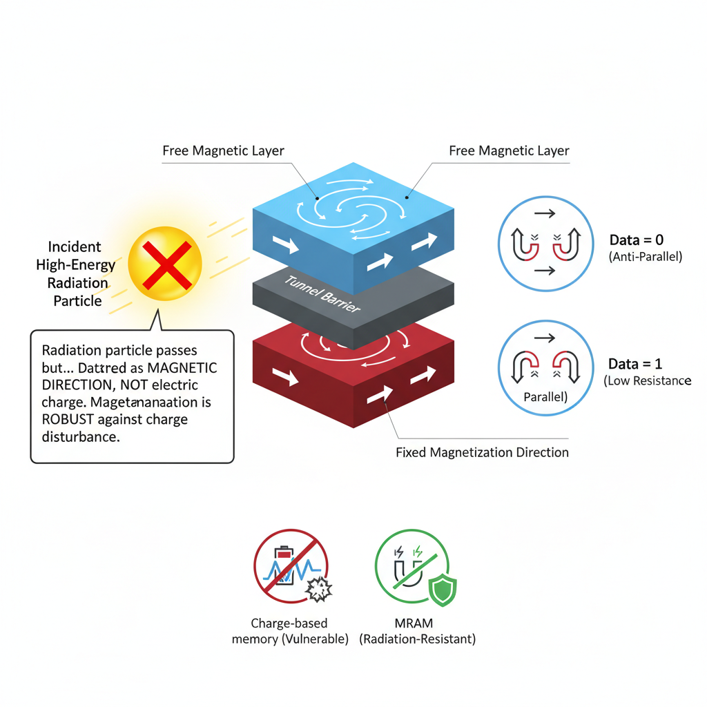
fact MRAM stores data through magnetic state rather than capacitor charge. That is why it behaves differently from SRAM and DRAM under radiation stress and why it can retain data with power removed. TC judgment For an aerospace designer, that physical difference only matters if it improves the actual system behavior. The premium is justified when the answer is yes.
2. Where MRAM fits best in the aerospace memory map
The most useful way to think about MRAM is not as a universal replacement for every memory type. It is better understood as a mission-memory middle layer between volatile high-speed memory and low-cost bulk non-volatile storage.
In practice, the strongest aerospace use cases usually cluster in four areas:
Boot and configuration memory
Space and aviation systems often need configuration data, calibration constants, and boot-critical information to survive unexpected resets. fact A memory that retains data without refresh and can be rewritten without erase-block management reduces the amount of firmware work needed to protect those assets. TC judgment This is one of the cleanest justifications for MRAM because the commercial value is easy to explain: less recovery logic, fewer write-management edge cases, and faster restart behavior.
Event logging and black-box style retention
Event logging is where flash can become awkward. The write path may need erase planning, wear management, or buffering logic to avoid losing the last useful state during a brownout or fault event. TC judgment MRAM earns attention here because the system can keep writing persistent state with much less firmware ceremony. If the mission cares about the last fault code, the last telemetry snapshot, or the last actuator command before reset, MRAM is often easier to justify than a flash-only architecture.
Fast restart and instant-on subsystems
Some aerospace electronics care as much about recovery time as they do about raw memory density. A subsystem that can re-enter service quickly after a power interruption, watchdog event, or radiation upset may benefit from persistent working data that does not require a slow rebuild sequence. inference This is one reason MRAM frequently appears in discussion around control electronics, supervisory processing, and embedded mission-support logic rather than payload-class mass storage.
High-write persistent state
Mission systems that repeatedly update counters, health records, learned calibration values, or runtime checkpoints need write endurance, not just retention. fact MRAM is commonly valued for very high write-cycle capability. TC judgment This makes it commercially relevant in long-life aerospace and defense electronics where memory wear-out planning itself becomes a program-management burden.
3. What radiation tolerance does and does not solve
This is the part many older articles oversimplify.
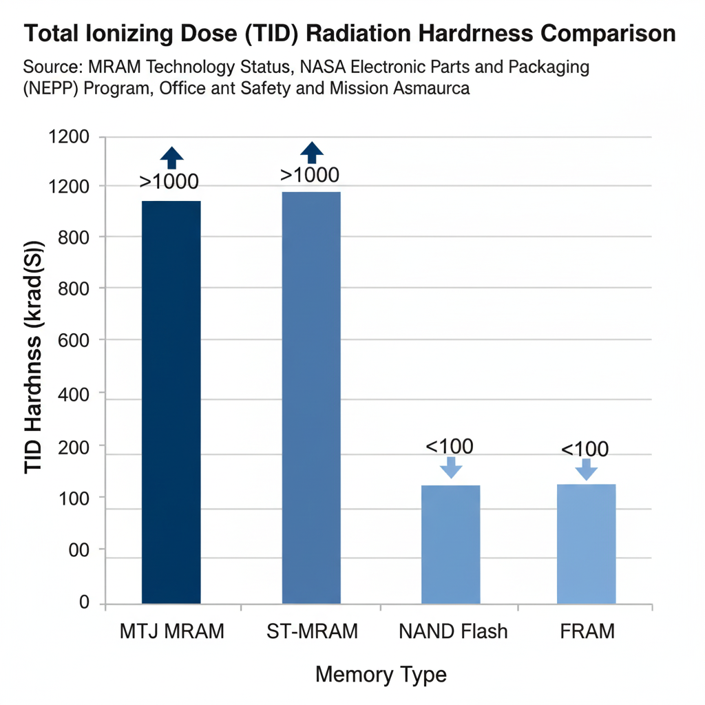
fact Because MRAM cells store information magnetically, they are less exposed to the charge-disturbance mechanism that drives many SRAM or DRAM upset concerns. That is a real advantage. It is also only half the story.
fact The surrounding CMOS circuitry still matters. Address decoding, control logic, I/O structures, package parasitics, board layout, shielding posture, power quality, and system-level error handling all remain part of the radiation discussion. TC judgment A buyer should never read "MRAM is radiation tolerant" as "the memory subsystem no longer needs qualification."
The practical boundary is below:
| Question | Better answer |
|---|---|
| Are MRAM cells generally more resilient than charge-based cells? | Yes, that is one of the technology's core attractions. |
| Does that make every MRAM device automatically suitable for space or flight hardware? | No, not without mission-specific evidence and system-level review. |
| Should buyers ask for radiation data, qualification notes, or program history? | Yes, especially when the part is intended for harsh-environment deployment. |
| Does board architecture still matter? | Absolutely. A resilient memory cell does not replace resilient system design. |
TC judgment For aerospace procurement, the safe reading is: MRAM can reduce one class of memory weakness, but it does not eliminate validation work.
4. Why MRAM is often chosen over flash in mission-support electronics
If the design only needs cheap non-volatile capacity, flash often wins. If the design needs persistent writes with less housekeeping, MRAM becomes much more compelling.
The decision usually turns on firmware burden and recovery behavior:
| Design concern | Flash-centered answer | MRAM-centered answer |
|---|---|---|
| Frequent writes | Needs wear planning and erase management | Easier persistent-write behavior |
| Brownout or sudden power loss | Often needs extra write-protection logic | Better fit for preserving the latest state |
| Fast restart | May require more recovery reconstruction | Persistent working data is easier to retain |
| Cost per bit | Usually better | Usually worse |
| Density | Usually higher | Usually lower |
TC judgment That table explains why MRAM is attractive in aerospace control logic but less attractive as a blanket replacement for payload or archive storage. The value is not density. The value is state retention with less drama.
5. Why Everspin still matters in the commercial supply conversation
Discrete MRAM is still a narrower market than commodity EEPROM, NOR flash, or DRAM. fact That means buyers usually evaluate a shorter list of recognized suppliers when they need standalone MRAM devices. Everspin remains one of the strongest commercial reference points in that discussion because the company is closely associated with discrete MRAM rather than only embedded MRAM inside a larger SoC.
TC judgment This matters even for aerospace-adjacent programs that are not buying flight-qualified memory directly. Lab evaluation, engineering validation, environmental testing, and industrial-to-aerospace transition work often begin with commercially visible discrete parts. A known commercial anchor makes that process easier to manage.
The MR25H40CDF is a useful example. It is not "space memory" by label alone, and this article is not claiming it should be dropped directly into a flight design. What it does show is the commercial side of the market: a discrete SPI MRAM device that helps teams evaluate persistent-write behavior, non-volatility, and lifecycle planning before they commit to a wider architecture.
6. The buyer checklist before qualifying MRAM for aerospace work
The procurement conversation should be more disciplined than "MRAM sounds safer."
Use this review stack before approving a device:
- Confirm the memory role: boot, event log, persistent working data, or bulk storage.
- Verify whether the design needs high write endurance, instant-on behavior, or brownout-safe persistence strongly enough to justify the MRAM premium.
- Review radiation evidence at the device and subsystem level instead of relying on a technology-category claim.
- Check interface fit: SPI, QSPI, parallel bus, density, voltage, package, and thermal assumptions.
- Ask for lifecycle posture, supply continuity, and whether the part is being treated as a lab-evaluation anchor or an approved production memory.
- Separate commercial discrete MRAM sourcing from mission qualification. They are related, but they are not the same step.
TC judgment That last point is where many early-stage teams lose clarity. A part can be commercially available and technically interesting while still requiring significant qualification work before it belongs in a harsh-environment release.
7. When MRAM is the wrong answer
MRAM should not be treated as a prestige technology that automatically upgrades a design.
It is usually the wrong answer when:
- the application mainly needs the lowest cost per bit
- the design stores large payload datasets where density dominates the decision
- the firmware already handles flash wear and recovery cleanly
- the qualification budget cannot support a specialized memory review
TC judgment Aerospace programs win by using specialized parts only where the mission benefit is real. MRAM is strongest when the memory job is persistence-heavy, recovery-sensitive, and reliability-driven. Outside that zone, conventional memory can remain the better commercial decision.
Bottom line
MRAM matters in aerospace because it can simplify some of the hardest memory behaviors: repeated persistent writes, fast recovery, and retention under power interruption. Its radiation posture is an advantage, but not a free pass. The right buyer question is not whether MRAM sounds advanced. The right question is whether this specific memory role becomes safer or simpler when the system stops depending on charge-based storage behavior.
If your team is reviewing discrete MRAM options such as MR25H40CDF, treat that part as a useful commercial anchor for architecture review and sourcing discussions, then pair it with the qualification evidence your mission profile actually requires.