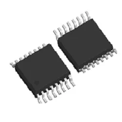
Supply original CD40109BPWR, Logic - Translators, Level Shifters, by texas

Pictures are for reference only. Please contact us for the latest pictures.
Availability
Price Range
| Quality | Unit Price |
|---|---|
| 1 | |
| 10 | |
| 30 | |
| 100 | |
| 500 | |
| 1,000 |
Due to different local policies, please contact us for the latest quotation.
We are ISO 9001, AS 9120B, IOS 14001 certified, ensuring that our quality management system meets international standards. This certification guarantees that every electronic component we supply is authentic, reliable, and traceable. Our dedicated inspection team conducts rigorous quality checks to prevent counterfeit products and reduce failure rates. By adhering to these stringent quality controls, we provide our customers with peace of mind and products they can trust.
Overview
The CD40109BMS, unlike other low-to-high level shifting circuits, does not require the presence of the high voltage supply (VDD) before the application of either the low voltage supply (VCC) or the input signals.
There are no restrictions on the sequence of application of VDD, VCC, or the input signals. In addition, with one exception there are no restrictions on the relative magnitudes of the supply voltages or input signals within the device maximum ratings, provided that the input signal swings between VSS and at least 0.7VCC; VCC may exceed VDD, and input signals may exceed VCC and VDD. When operated in the mode VCC > VDD, the CD40109BMS will operate as a high-to-low level shifter.
Features
• High Voltage Type (20V Rating)
• Independence of Power Supply Sequence Considerations - VCC can Exceed VDD - Input Signals can Exceed Both VCC and VDD
• Up and Down Level Shifting Capability
• Three-State Outputs with Separate Enable Controls
• 100% Tested for Quiescent Current at 20V
• 5V, 10V and 15V Parametric Ratings
• Maximum Input Current of 1µA at 18V Over Full Package Temperature Range; 100nA at 18V and +25oC
• Noise Margin (Over Full Package/Temperature Range) - 1V at VCC = 5V, VDD = 10V - 2V at VCC = 10V, VDD = 15V
• Standardized Symmetrical Output Characteristics
• Meets All Requirements of JEDEC Tentative Standard No. 13B, “Standard Specifications for Description of ‘B’ Series CMOS Devices”Applications
• High or Low Level Shifting with Three-State Outputs for Unidirectional or Bidirectional Bussing
• Isolation of Logic Subsystems Using Separate Power Supplies from Supply Sequencing, Supply Loss and Supply Regulation Considerations
Product Attribute
Export Classifications & Environmental
Product Parameter
Articles
This guide provides a direct comparison of HBM generations (up to HBM3e), analyzes the market landscape dominated by SK Hynix, Samsung, and Micron, and offers a crucial procurement checklist. It concludes with a practical case study, advising on capacity and bandwidth requirements (e.g., for a 175B parameter LLM), ensuring businesses can make informed decisions for their high-performance AI systems.
The Nexperia geopolitical crisis, involving legal takeover and counter-sanctions, poses the most severe recent risk to the global semiconductor supply chain, demanding immediate analysis of supply bottlenecks and price impacts for all component buyers.
With its unique properties of radiation hardening, unlimited read/write endurance, and low power consumption, MRAM is becoming the preferred choice for next-generation aerospace memory. This article will provide an in-depth analysis of MRAM's key advantages and applications in the aerospace field.
Comprehensive overview of MR25H40CDF SPI MRAM: specs, applications, case studies, and our real-stock advantages.
