
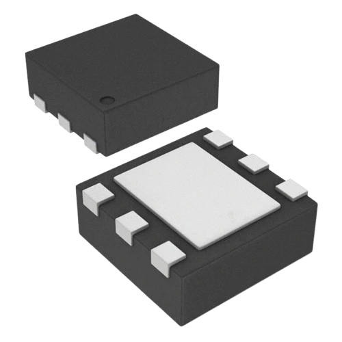
MR25H40CDF Toggle MRAM by Everspin Technologies
MR25H40CDF is a Toggle MRAM from Everspin Technologies in DFN EP packaging. It is commonly reviewed for MRAM 4Mbit Serial-SPI Interface 3.3V. This page lists current TrustCompo stock, tier pricing, package data, datasheet access, compliance attributes, Hong Kong warehouse shipping options, payment confirmation, and RFQ options for buyers verifying this exact ordering code.
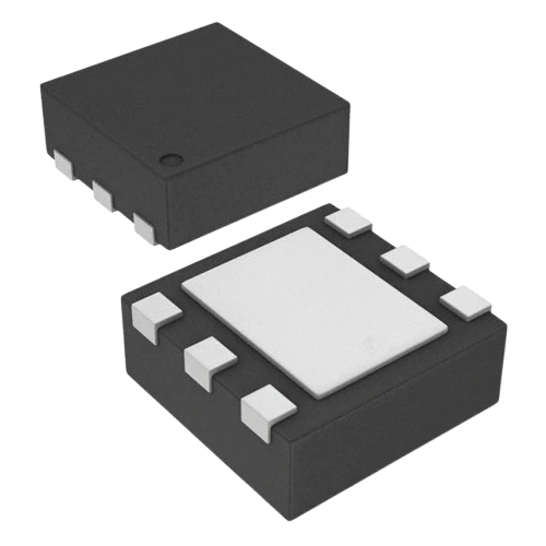
Pictures are for reference only. Please contact us for the latest pictures.
- 365-Day GuaranteeAfter-sales support helps buyers handle quality questions with a clearer return and review window.
- Ships within 24-48 HoursAvailable items can move quickly once the quote, quantity, and delivery details are confirmed.
- 100% Anti-Counterfeit TestedParts are checked through authenticity-focused handling and inspection before shipment.
Key specifications
- Part Number
MR25H40CDF
- Internal code
TCE000012979
- Package
DFN EP
- Manufacturer
- Everspin Technologies
Key specifications
- Series
MR2xH40
- Min Quantity
1
- Category
- MRAM
- Sub Category
- Toggle MRAM
- Description
MRAM 4Mbit Serial-SPI Interface 3.3V
- key Attributes
-
- Datasheet
- View MR25H40CDF Datasheet
Trust signals
Quality and trust signals
Review TrustCompo quality credentials, traceability support, anti-counterfeit handling, and inspection controls before sending an RFQ.
4 certifications
ISO 9001
Quality management processes for more consistent sourcing and handling.
AS9120B
Aerospace-focused distribution controls for traceability and reliability.
ISO 14001
Environmental management discipline across warehouse and operating workflows.
ESD Control
Electrostatic handling standards to help protect sensitive components.
RFQ checklist
Order process
Confirm the core buying details for MR25H40CDF before RFQ, PO release, and shipment planning.
- 1
Confirm MPN
Use the exact part number, manufacturer, package, and approval constraints in the RFQ.
- 2
Check stock and price
Verify live availability, MOQ, lead time, final unit price, and tax terms before PO release.
- 3
Align documents
Confirm datasheet, CoC, traceability, lifecycle notes, and inspection scope when required.
- 4
Arrange shipment
Release the PO and align DHL, FedEx, UPS, or buyer forwarder shipment from Hong Kong.
Before PO release
Part confirmation
- Exact MPN confirmed: MR25H40CDF
- Package to verify: DFN EP
Commercial confirmation
- Live stock and lead time confirmed by RFQ
- Final price and tax terms confirmed before PO release
Fulfillment & documents
- Ship-from location: Hong Kong warehouse
- Shipping method: DHL, FedEx, UPS, or buyer forwarder account
Product overview
Product overview
Review the sourcing context for MR25H40CDF from Everspin Technologies, including product identity, application fit, package notes, and purchasing considerations.
MR2xH40 is a family of 4,194,304-bit magnetoresistive random access memory (MRAM) devices organized as 524,288 words of 8 bits. They are the ideal memory solution for applications that must store and retrieve data and programs quickly using a small number of I/O pins. They have serial EEPROM and serial Flash compatible read/write timing with no write delays and unlimited read/write endurance. Unlike other serial memories, with the MR2xH40 family both reads and writes can occur randomly in memory with no delay between writes. The MR2xH40 family provides highly reliable data storage over a wide range of temperatures. The MR20H40 (50MHz) is offered with Industrial (-40° to +85 °C) range. The MR25H40 (40MHz) is offered with Industrial (-40 to +85 °C), Extended (-40 to 105°C), and AEC-Q100 Grade 1 (-40°C to +125 °C) operating temperature range options. Both are available in a 5 x 6mm, 8-pin DFN package. The pinout is compatible with serial SRAM, EEPROM, Flash, and FeRAM products.
Technical parameters
Parameters
Compare grouped MR25H40CDF parameters from Everspin Technologies, including package, series, key attributes, and technical values used for engineering and sourcing review.
Product Attribute
Part Status
Active
Product Attribute
Max Access Time
9
Product Attribute
Data Bus Width
8
Product Attribute
Pin Count
8
Product Attribute
Operating Current
42
Product Attribute
Chip Density (Bit)
4M
| Parameter | Value |
|---|---|
Part Status Lifecycle status of the part, such as active or obsolete. Indicates availability and long-term support from the manufacturer. Check this before design-in to avoid last-time buys or supply disruptions. Verify with the datasheet or distributor for current status. | Active |
Max Access Time Maximum time from address or control signal to valid data output. Critical for memory speed and system timing. Compare with your required cycle time and verify against datasheet for worst-case conditions. | 9 |
Data Bus Width Specifies the number of bits transferred simultaneously on the data bus. This affects data throughput and interface compatibility. Verify against the datasheet to ensure the device matches your system's bus architecture and performance requirements. | 8 |
Pin Count Total number of pins or terminals on the component package. Essential for footprint design, PCB layout, and connector mating. Verify against the datasheet to ensure compatibility with your board and assembly process. | 8 |
Operating Current Typical current drawn by the component during normal operation. Compare this value with your power budget and check the datasheet for maximum ratings and variations across supply voltage and load conditions. | 42 |
Chip Density (Bit) Total memory capacity of the chip in bits. Compare this value to your application's storage requirements. Verify against the datasheet to ensure the exact density and organization match your design. | 4M |
Operating Temperature Range Specifies the minimum and maximum ambient temperatures at which the component operates reliably. Compare this range with your application's thermal environment to ensure performance and longevity. Always verify against the datasheet for derating curves and absolute maximum ratings. | -40°C to +85°C |
Interface Type Specifies the communication protocol used by the component to exchange data with a host controller or other devices. Common examples include I2C, SPI, UART, USB, and CAN. Verify compatibility with your system's bus architecture and voltage levels before integration. | Serial-SPI |
Memory Organization Specifies the internal arrangement of memory cells, typically expressed as words by bits. This affects how data is accessed and stored. Engineers compare this to ensure compatibility with their system's bus width and addressing scheme. Always verify against the datasheet for exact configuration. | 512Kx8 |
Operating Voltage Specifies the supply voltage range within which the component functions correctly. Engineers compare this to the system's power rails to ensure compatibility. Always verify the absolute maximum ratings in the datasheet to prevent damage from overvoltage or undervoltage conditions. | 3.3 (3 to 3.6) |
Endurance Indicates the number of program/erase cycles a memory device can withstand before performance degrades. This is critical for flash and EEPROM in applications with frequent writes. Engineers compare endurance to ensure data retention and reliability over the product's lifetime. Verify the specified endurance rating in the datasheet. | Unlimited |
Timing Compatibility Describes whether the component's timing parameters align with industry-standard specifications, such as JEDEC or specific bus protocols. This ensures interoperability with other devices in a system. Engineers must verify timing compatibility to avoid data corruption or system failures. Check the datasheet for timing diagrams and compliance statements. | Serial EEPROM/Flash |
| Parameter | Value |
|---|---|
Mounting Defines the physical mounting method for the component, such as surface mount, through-hole, or chassis mount. This determines PCB layout, assembly process, and mechanical stability. Buyers must match mounting type to their manufacturing capabilities and application environment. Check the datasheet for recommended footprint and soldering profile. | Surface Mount |
Lead Shape Indicates the physical configuration of component leads, such as gull-wing, J-lead, or through-hole. This affects PCB footprint design, soldering process, and mechanical reliability. Verify against the package drawing to ensure compatibility with your assembly line and layout. | NO LEAD |
Package Dimensions Physical dimensions of the component package, typically length, width, and height. Essential for PCB layout and mechanical design. Compare with the datasheet to ensure proper fit and clearance in your application. | 6.1 x 5.1 x 0.95 mm (Max) |
Supplier Package Package name as designated by the manufacturer, such as SOIC-8 or QFN-32. Use this to identify the exact package variant and footprint. Cross-reference with the datasheet for pin layout and thermal pad details. | DFN EP |
Pinout Compatibility Indicates whether the component's pin configuration matches standard or existing footprints, allowing drop-in replacement without PCB redesign. This is crucial for second-source sourcing and design flexibility. Engineers compare pinouts to ensure compatibility with existing layouts. Verify the pinout diagram in the datasheet before design-in. | Serial SRAM/EEPROM/Flash/FeRAM |
| Parameter | Value |
|---|---|
PPAP Indicates whether Production Part Approval Process documentation is available for this component. Buyers and engineers should verify PPAP availability when sourcing parts for automotive or safety-critical applications to ensure supplier quality and traceability. | NO |
Automotive Indicates qualification for automotive applications, typically meeting AEC-Q standards and extended temperature ranges. Essential for designs requiring high reliability under harsh conditions. Confirm specific grade and certifications in the datasheet. | NO |
EU RoHS Indicates whether the component complies with the EU Restriction of Hazardous Substances directive. Check this attribute to ensure regulatory compliance for products sold in the European market. Verify against the latest RoHS certificate or datasheet. | Compliant |
ECCN (US) The US Export Control Classification Number determines export licensing requirements for electronic components. Verify the current ECCN from the manufacturer or datasheet, as it affects international shipping and compliance with US regulations. | EAR99 |
Datasheet preview
Datasheet PDF viewer
Preview the MR25H40CDF datasheet from Everspin Technologies to check package, electrical characteristics, application notes, and document evidence before RFQ.
Everspin Technologies
MR25H40CDF
Page 1 of 0 / —
Loading PDF viewer...
Notice documents
PCN / product notice documents
0 documents
No public PCN / PDN records currently displayed
No public product notice document is currently displayed for MR25H40CDF. Confirm PCN, PDN, EOL, date code, and lifecycle status during RFQ before production purchase.
Related sourcing options
Recommended products
Explore related Toggle MRAM products to compare fit, stock status, datasheets, and sourcing options.




Common questions
Product FAQ
Targeted answers for buyers verifying the exact MR25H40CDF ordering code, packaging, stock, datasheet, and replacement path.
What does MR25H40CDF mean?
MR25H40CDF is the exact ordering code listed for a Toggle MRAM component from Everspin Technologies. The current package reference is DFN EP, with listed context including MRAM 4Mbit Serial-SPI Interface 3.3V. Buyers should use the full code when requesting stock, price, datasheet, or compliance confirmation.
How should buyers verify the MR25H40CDF ordering code?
Treat MR25H40CDF as the full ordering code during RFQ and engineering review. Confirm the listed DFN EP package, manufacturer documentation from Everspin Technologies, datasheet ordering table, reel or packing details, and any customer approval constraints before substitution or PO release.
What package is MR25H40CDF supplied in?
MR25H40CDF is currently listed with package reference DFN EP from Everspin Technologies. Buyers should confirm the manufacturer package drawing, footprint, pinout, tape-and-reel details, and receiving requirements before approval.
Is MR25H40CDF currently available?
MR25H40CDF is currently marked with stock availability on this page. Before ordering, confirm the package (DFN EP), listed stock (127887), available quantity (48109), required quantity, lead time, final price, compliance needs, and exact ordering code match through RFQ.
Where can I compare MR25H40CDF alternatives?
A mapped alternative list is not currently published for MR25H40CDF. Send an RFQ with the target quantity, package constraints, and approval requirements so TrustCompo can help review credible replacement options.