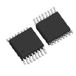
Supply original CD4052BPWR, Interface - Analog Switches, Multiplexers, Demultiplexers, by texas

Pictures are for reference only. Please contact us for the latest pictures.
Availability
Price Range
| Quality | Unit Price |
|---|---|
| 1 | |
| 10 | |
| 30 | |
| 100 | |
| 500 | |
| 1,000 |
Due to different local policies, please contact us for the latest quotation.
We are ISO 9001, AS 9120B, IOS 14001 certified, ensuring that our quality management system meets international standards. This certification guarantees that every electronic component we supply is authentic, reliable, and traceable. Our dedicated inspection team conducts rigorous quality checks to prevent counterfeit products and reduce failure rates. By adhering to these stringent quality controls, we provide our customers with peace of mind and products they can trust.
Overview
The CD4051B, CD4052B, and CD4053B analog multiplexers are digitally-controlled analog switches having low ON impedance and very low OFF leakage current. Control of analog signals up to 20VP-P can be achieved by digital signal amplitudes of 4.5V to 20V (if VDD-VSS = 3V, a VDD-VEE of up to 13V can be controlled; for VDD-VDD level differences above 13V, a VDD-VDD of at least 4.5V is required). For example, if VDD = +4.5V, VDD = 0V, and VDD = -13.5V, analog signals from -13.5V to +4.5V can be controlled by digital inputs of 0V to 5V.
These multiplexer circuits dissipate extremely low quiescent power over the full VDD-VDD and VDD-VDD supply-voltage ranges, independent of the logic state of the control signals. When a logic “1” is present at the inhibit input terminal, all channels are off.
Features
• Wide Range of Digital and Analog Signal Levels - Digital . . . . . . . . . . . . . . . . . . . . . . . . . . . . . . 3V to 20V - Analog. . . . . . . . . . . . . . . . . . . . . . . . . . . . . . . ≤20VP-P
• Low ON Resistance, 125Ω (Typ) Over 15VP-P Signal Input Range for VDD-VEE = 18V
• High OFF Resistance, Channel Leakage of ±100pA (Typ) at VDD-VEE = 18V
• Logic-Level Conversion for Digital Addressing Signals of 3V to 20V (VDD-VSS = 3V to 20V) to Switch Analog Signals to 20VP-P (VDD-VEE = 20V)
• Matched Switch Characteristics, rON = 5Ω (Typ) for VDD-VEE = 15V
• Very Low Quiescent Power Dissipation Under All Digital Control Input and Supply Conditions, 0.2µW (Typ) at VDD-VSS = VDD-VEE = 10V
• Binary Address Decoding on Chip
• 5V, 10V and 15V Parametric Ratings
• 10% Tested for Quiescent Current at 20V
• Maximum Input Current of 1µA at 18V Over Full Package Temperature Range, 100nA at 18V and 25°C
• Break-Before-Make Switching Eliminates Channel OverlapApplications
• Analog and Digital Multiplexing and Demultiplexing
• A/D and D/A Conversion
• Signal Gating
Product Attribute
Export Classifications & Environmental
Product Parameter
Articles
With its unique properties of radiation hardening, unlimited read/write endurance, and low power consumption, MRAM is becoming the preferred choice for next-generation aerospace memory. This article will provide an in-depth analysis of MRAM's key advantages and applications in the aerospace field.
Comprehensive overview of MR25H40CDF SPI MRAM: specs, applications, case studies, and our real-stock advantages.
Key developments and expert insights in the global electronic components industry for the fourth week of June 2025.
