
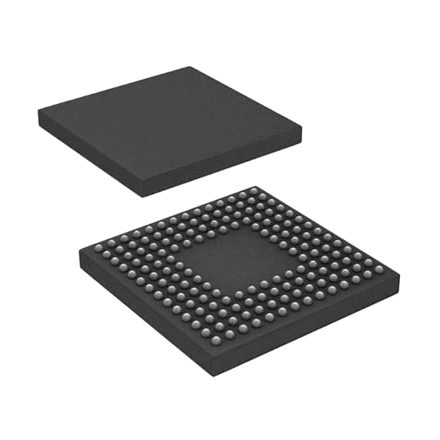
XC5VLX50T-1FFG665C Embedded - FPGAs (Field Programmable Gate Array) by Xilinx
XC5VLX50T-1FFG665C is a Embedded - FPGAs (Field Programmable Gate Array) from Xilinx in BGA packaging. It is commonly reviewed for IC FPGA 360 I/O 665FCBGA. This page lists current TrustCompo stock, tier pricing, package data, datasheet access, compliance attributes, Hong Kong warehouse shipping options, payment confirmation, and RFQ options for buyers verifying this exact ordering code.
In StockDatasheet
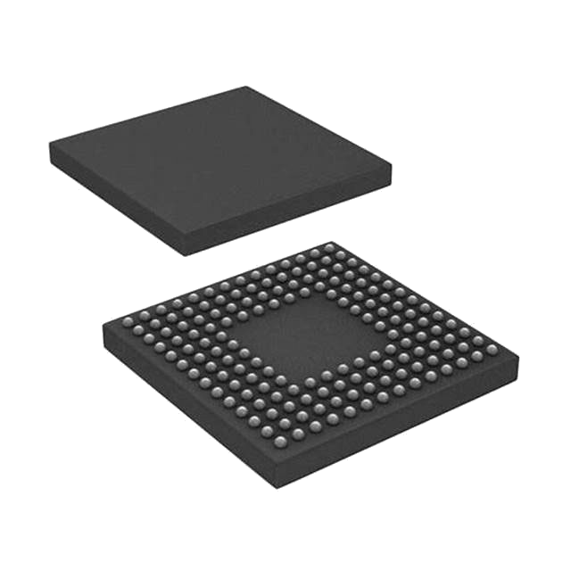
Pictures are for reference only. Please contact us for the latest pictures.
- 365-Day GuaranteeAfter-sales support helps buyers handle quality questions with a clearer return and review window.
- Ships within 24-48 HoursAvailable items can move quickly once the quote, quantity, and delivery details are confirmed.
- 100% Anti-Counterfeit TestedParts are checked through authenticity-focused handling and inspection before shipment.
Key specifications
- Part Number
XC5VLX50T-1FFG665C
- Internal code
TCE000120624
- Package
BGA
- Manufacturer
- Xilinx
Key specifications
- Series
Virtex®-5 LXT
- Min Quantity
1
- Category
- Integrated Circuits (ICs)
- Sub Category
- Embedded - FPGAs (Field Programmable Gate Array)
- Description
IC FPGA 360 I/O 665FCBGA
- key Attributes
-
- Datasheet
- View XC5VLX50T-1FFG665C Datasheet
Trust signals
Quality and trust signals
Review TrustCompo quality credentials, traceability support, anti-counterfeit handling, and inspection controls before sending an RFQ.
4 certifications
ISO 9001
Quality management processes for more consistent sourcing and handling.
AS9120B
Aerospace-focused distribution controls for traceability and reliability.
ISO 14001
Environmental management discipline across warehouse and operating workflows.
ESD Control
Electrostatic handling standards to help protect sensitive components.
RFQ checklist
Order process
Confirm the core buying details for XC5VLX50T-1FFG665C before RFQ, PO release, and shipment planning.
- 1
Confirm MPN
Use the exact part number, manufacturer, package, and approval constraints in the RFQ.
- 2
Check stock and price
Verify live availability, MOQ, lead time, final unit price, and tax terms before PO release.
- 3
Align documents
Confirm datasheet, CoC, traceability, lifecycle notes, and inspection scope when required.
- 4
Arrange shipment
Release the PO and align DHL, FedEx, UPS, or buyer forwarder shipment from Hong Kong.
Before PO release
Part confirmation
- Exact MPN confirmed: XC5VLX50T-1FFG665C
- Package to verify: BGA
Commercial confirmation
- Live stock and lead time confirmed by RFQ
- Final price and tax terms confirmed before PO release
Fulfillment & documents
- Ship-from location: Hong Kong warehouse
- Shipping method: DHL, FedEx, UPS, or buyer forwarder account
Product overview
Product overview
Review the sourcing context for XC5VLX50T-1FFG665C from Xilinx, including product identity, application fit, package notes, and purchasing considerations.
24-BIT DIGITAL SIGNAL PROCESSOR
The Motorola DSP56307, a member of the DSP56300 family of programmable digital signal processors (DSPs), supports wireless infrastructure applications with general filtering operations.
The on-chip enhanced filter coprocessor (EFCOP) processes filter algorithms in parallel with core operation, thus increasing overall DSP performance and efficiency. Like the other family members, the DSP56307 uses a high-performance, single-clock-cycle-per-instruction engine (code-compatible with Motorolas popular DSP56000 core family), a barrel shifter, 24-bit addressing, an instruction cache, and a direct memory access controller, as in Figure 1.
The DSP56307 offers performance at 100 million instructions (MIPS) per second using an internal 100 MHz clock with a 2.5 volt core and independent 3.3 volt input/output power.
FEATURESHigh-Performance DSP56300 Core● 100 million instructions per second (MIPS) with a 100 MHz clock at 2.5 V core and 3.3 V I/O● Object code compatible with the DSP56000 core● Highly parallel instruction set● Data arithmetic logic unit (ALU) - Fully pipelined 24 x 24-bit parallel multiplier-accumulator - 56-bit parallel barrel shifter (fast shift and normalization; bit stream generation and parsing) - Conditional ALU instructions - 24-bit or 16-bit arithmetic support under software control● Program control unit (PCU) - Position independent code (PIC) support - Addressing modes optimized for DSP applications (including immediate offsets) - On-chip instruction cache controller - On-chip memory-expandable hardware stack - Nested hardware DO loops - Fast auto-return interrupts● Direct memory access (DMA) - Six DMA channels supporting internal and external accesses - One-, two-, and three- dimensional transfers (including circular buffering) - End-of-block-transfer interrupts - Triggering from interrupt lines and all peripherals● Phase-locked loop (PLL) - Allows change of low power divide factor (DF) without loss of lock - Output clock with skew elimination● Hardware debugging support - On-Chip Emulation (OnCE) module - Joint test action group (JTAG) test access port (TAP) - Address trace mode reflects internal Program RAM accesses at the external port
Technical parameters
Parameters
Compare grouped XC5VLX50T-1FFG665C parameters from Xilinx, including package, series, key attributes, and technical values used for engineering and sourcing review.
Product Parameter
Triac Type
Active
Product Parameter
Typical Quiescent Current (MA)
CMOS
Product Parameter
Transformer Type
yes
Product Parameter
On-State Resistance Match-Nom
Not Qualified
Product Parameter
Total Resistance
Tray
Product Parameter
Nominal Attenuation
e1
| Parameter | Value |
|---|---|
Triac Type Specifies the triac construction or series, such as standard, snubberless, or logic-level. This affects switching performance, gate sensitivity, and commutation capability. Verify the exact type against the datasheet to ensure compatibility with your circuit's voltage, current, and triggering requirements. | Active |
Typical Quiescent Current (MA) Typical current consumed by the component in standby or idle state, measured in milliamperes. This is important for battery-powered or low-power applications. Compare this value with your power budget to ensure the component does not drain excessive current when inactive, affecting overall system efficiency. | CMOS |
Transformer Type Indicates the construction or configuration of the transformer, such as flyback, forward, or planar. Affects performance, size, and application suitability. Refer to datasheet for detailed specifications and recommended usage. | yes |
On-State Resistance Match-Nom Indicates the nominal matching of on-state resistance between multiple channels in a device, such as a dual MOSFET or analog switch. This parameter is critical for parallel operation and current sharing. Verify the specified match against the datasheet to ensure balanced performance. | Not Qualified |
Total Resistance Total resistance is the end-to-end resistance of a component, such as a potentiometer or resistor network. It defines the maximum resistance available and is critical for circuit design. Verify this value against the datasheet to ensure proper operation. | Tray |
Nominal Attenuation Specifies the typical signal loss introduced by the component under standard conditions. Compare this value across similar parts to match your circuit's allowable attenuation. Always verify against the datasheet for frequency and temperature dependencies. | e1 |
Accessory Type Specifies the category of accessory or add-on part for electronic components. Use this to filter compatible mounting hardware, connectors, or protective covers. Verify the accessory type against the component datasheet to ensure proper fit and function in your application. | BOTTOM |
Minimum Operating Supply Voltage Specifies the lowest supply voltage at which the component remains fully functional. Compare this value with your system's power rail tolerance and verify it against the datasheet's recommended operating conditions to ensure reliable startup and operation. | BALL |
Voltage Rating Specifies the maximum continuous voltage the component can safely withstand without damage or performance degradation. Critical for ensuring proper operating margins in power supplies, signal lines, and isolation barriers. Always confirm with the datasheet for absolute maximum ratings. | 30 |
Number Of Turns Number of turns in a coil or winding. Affects inductance, transformer ratio, and impedance. Critical for designing transformers, inductors, and magnetic components. Check datasheet for tolerance. | 27mm |
Taper Specifies the resistance change curve of a potentiometer, such as linear or logarithmic. This affects how the output varies with rotation. Verify the taper type against your circuit requirements and the datasheet to ensure proper volume or control response. | 2.4mm |
Maximum Operating Supply Voltage Highest supply voltage at which the component can operate normally without damage or performance degradation. Exceeding this limit may cause overheating or failure. Always check this parameter against your power supply design to ensure the component operates within its safe voltage range for reliable long-term performance. | 250 |
Typical Switching Frequency (KHz) Typical switching frequency of a power converter or driver. Compare this value to your application's needs to ensure efficient operation. Verify against the datasheet for exact conditions. | Field Programmable Gate Arrays |
Speed Grade Speed grade indicates the maximum operating frequency or propagation delay category for digital ICs, memory, or programmable logic. Compare grades when selecting parts for timing-critical designs. Verify the exact speed rating in the datasheet to ensure it meets your system's clock and signal integrity requirements. | 1 |
Collector-Emitter Voltage-Max Maximum voltage that can be applied between collector and emitter without breakdown. Critical for BJT and IGBT selection. Verify against datasheet to ensure safe operation within your circuit's supply and transient conditions. | FIELD PROGRAMMABLE GATE ARRAY |
Capacitance Capacitance value of the component, typically expressed in farads (pF, nF, µF). This parameter determines energy storage and filtering characteristics. Compare capacitance when selecting capacitors for power supply decoupling, signal coupling, or timing applications. Always check the rated voltage and tolerance in the datasheet. | 360 |
Number Of LABs/CLBs Indicates the count of logic array blocks or configurable logic blocks in an FPGA or CPLD. This metric helps compare logic capacity and complexity across devices. Verify against the datasheet for your specific design requirements. | 3600 |
Filter Type Specifies the filter topology used in the component, such as low-pass, high-pass, band-pass, or notch. This determines the frequency response and attenuation characteristics. Engineers must verify the filter type against the datasheet to ensure it meets the required signal conditioning and interference rejection for the application. | 665 |
Output High Voltage-Min Specifies the minimum voltage level that the output can drive when in a high logic state. Compare this value with the input high threshold of the receiving device to ensure proper logic compatibility. Verify against the datasheet for your operating conditions. | 2211840 |
Number Of Logic Elements/Cells Indicates the total count of programmable logic elements or cells in the FPGA or CPLD. This parameter determines the device's logic capacity and complexity. Compare this value with your design requirements to ensure sufficient resources. Always verify against the datasheet for exact specifications. | 46080 |
Transmission Media Type Specifies the physical medium through which signals travel, such as fiber optic, twisted pair, or coaxial cable. This attribute is critical for ensuring compatibility with your network infrastructure and for meeting performance requirements. Verify the media type against your system's specifications and the component datasheet to avoid signal integrity issues. | 1V |
Power Supplies Specifies the required power supply voltages for the component. Engineers use this to ensure the board's power rails match the device's needs. Verify against the datasheet's recommended operating conditions to avoid undervoltage or overvoltage issues. | Virtex®-5 LXT |
Terminal Block Type Specifies the mechanical configuration of the terminal block, such as pluggable, fixed, or barrier style. This affects mounting, wiring, and compatibility with mating connectors. Verify the exact type against the datasheet to ensure proper fit and reliable electrical connections in your assembly. | 270kB |
| Parameter | Value |
|---|---|
Categories Lists the product categories or classifications assigned to this component, such as connectors, capacitors, or modules. This helps in filtering and comparing similar parts. Review the categories to ensure the component fits your application and to find alternative parts in the same class. | Integrated Circuits (ICs) |
Housing Material Specifies the material of the component's outer casing, such as plastic, metal, or ceramic. This affects durability, thermal performance, and environmental resistance. Verify against datasheet for application-specific requirements like flammability or chemical exposure. | ROHS3 Compliant |
Terminal Position Position of the terminals on the package, such as dual-in-line, gull-wing, or J-lead. This affects PCB layout, soldering, and thermal performance. Engineers must ensure the terminal position matches the footprint and assembly capabilities of their manufacturing line. | Surface Mount |
Max Supply Voltage Indicates the highest DC or AC voltage that can be safely applied to the power supply pin without risking damage or malfunction. Verify this limit against the datasheet before designing your circuit to ensure reliable operation under all conditions. | Surface Mount |
Number Of Contacts Total number of electrical contacts in the connector, which determines the maximum number of circuits that can be connected. This is a critical parameter for matching the connector to your wire harness requirements. Ensure the contact count aligns with your signal and power needs. | Unknown |
Converter Type Identifies the conversion architecture, such as ADC, DAC, or DC-DC. This determines the signal path, interface, and performance characteristics. Verify the type matches your system's analog or digital conversion needs before selecting the part. | 4 (72 Hours) |
Interface Type Specifies the communication protocol used by the component to exchange data with a host controller or other devices. Common examples include I2C, SPI, UART, USB, and CAN. Verify compatibility with your system's bus architecture and voltage levels before integration. | not_compliant |
Threshold Voltage The minimum gate-to-source voltage that makes the device start conducting. Compare this value across parts to ensure your drive circuit can reliably turn the switch on. Always verify against the datasheet for your operating temperature. | 27mm |
Sub-Categories Indicates the specific product subcategories or classifications within the broader component family. Helps narrow down search results and identify the exact type of component needed for your design. Review the subcategory to ensure compatibility with your application. | Embedded - FPGAs (Field Programmable Gate Array) |
Supply Voltage Specifies the nominal operating voltage that must be applied to the component for proper function. Verify this value against your system's power rail and the datasheet's absolute maximum ratings to ensure reliable operation and avoid damage. | 1999 |
Input Power-Max (CW) Indicates the maximum continuous wave input power the component can safely handle without damage or excessive distortion. Exceeding this limit may cause failure. Verify this value against your signal power and consider peak-to-average ratio in modulated systems. | 10 Weeks |
Manufacturer Identifies the company that designed and produced the component. Buyers often filter by manufacturer to ensure brand reliability, quality standards, and supply chain consistency. Verify the manufacturer against the datasheet and official packaging to avoid counterfeit parts. | Xilinx |
Radiation Hardening Indicates if the component is designed to withstand ionizing radiation in space, nuclear, or high-energy physics applications. Compare radiation-tolerant vs. radiation-hardened parts for mission-critical designs. Verify the total ionizing dose (TID) and single-event effect (SEE) ratings in the datasheet. | 0°C~85°C TJ |
Specifications Review the complete technical specifications for this electronic component, including electrical ratings, mechanical dimensions, and environmental limits. Verify these parameters against your application requirements and the manufacturer's datasheet to ensure compatibility and reliable operation. | Tin/Silver/Copper (Sn95.5Ag4.0Cu0.5) |
Number Of I/O Total number of input/output pins or channels available on the device. Determines connectivity and interface capability. Verify against your system requirements and datasheet to ensure sufficient I/O for your application. | 360 |
Number Of Macro Cells Indicates the total number of macro cells in a CPLD or FPGA, which determines the logic capacity and complexity of designs you can implement. Compare this value against your required logic functions and check the datasheet for exact architecture and routing constraints. | 330000 |
Temperature Coefficient Indicates how much a key parameter, such as voltage or resistance, changes per degree Celsius. Lower values mean better stability across temperature. Verify this against your operating temperature range to ensure consistent performance in your environment. | 0.95V~1.05V |
Temperature Grade Defines the operating temperature range classification for the component, such as commercial, industrial, or automotive. This indicates the environmental conditions the device can withstand. Ensure the grade matches your application's ambient temperature requirements. | 665 |
Data Rate Specifies the maximum data transfer rate the component can handle, typically in bits per second. Compare this value with your system's required throughput to ensure adequate bandwidth. Verify against the datasheet for exact conditions and supported protocols. | 665 |
Package / Case Physical package or case type of the component, defining its dimensions, mounting style, and thermal characteristics. Common types include SMD, through-hole, BGA, and QFN. Choose the package that fits your PCB layout and assembly process. Verify the exact package code in the datasheet for footprint compatibility. | 665-BBGA, FCBGA |
Manufacturer'S Part No. The unique part number assigned by the original component manufacturer. Use this to cross-reference datasheets, verify specifications, and ensure the exact component matches your design requirements. Always confirm the number against the manufacturer's official documentation. | XC5VLX50T-1FFG665C |
Series Indicates the product series or family, grouping components with similar design and specifications. Helps identify compatible parts and compare within a product line. Verify the series against the datasheet to ensure correct application. | Virtex®-5 LXT |
Technology Manufacturing technology or process used for the component, such as thin film, thick film, or semiconductor process. Affects performance, stability, and cost. Confirm the technology matches your application requirements and environmental conditions. | XC5VLX50 |
Datasheet preview
Datasheet PDF viewer
Preview the XC5VLX50T-1FFG665C datasheet from Xilinx to check package, electrical characteristics, application notes, and document evidence before RFQ.
Xilinx
XC5VLX50T-1FFG665C
Page 1 of 0 / —
Loading PDF viewer...
Notice documents
PCN / product notice documents
0 documents
No public PCN / PDN records currently displayed
No public product notice document is currently displayed for XC5VLX50T-1FFG665C. Confirm PCN, PDN, EOL, date code, and lifecycle status during RFQ before production purchase.
Related sourcing options
Recommended products
Explore related Embedded - FPGAs (Field Programmable Gate Array) products to compare fit, stock status, datasheets, and sourcing options.
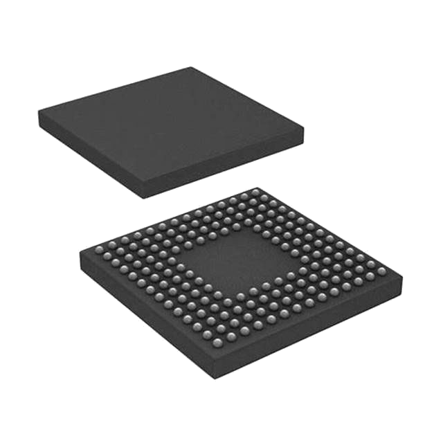 XC5VLX110T-1FFG1136I207 purchasedBGA带板In StockDatasheet
IC FPGA 640 I/O 1136FCBGA
Reference price$14.71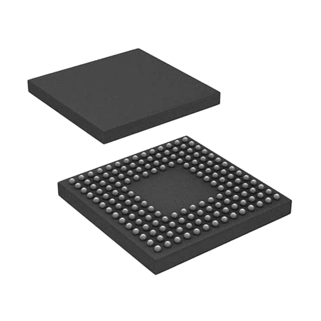 XC5VLX155T-1FFG1738I170 purchasedBGA带板In StockDatasheet
IC FPGA 680 I/O 1738FCBGA
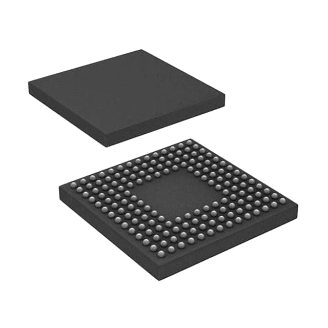
Reference price$5.00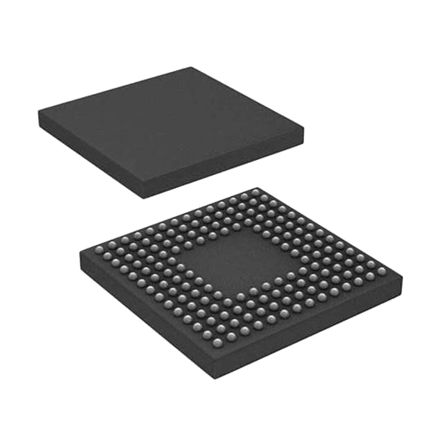 XC5VLX155T-1FFG1136I132 purchasedBGA带板In StockDatasheet
IC FPGA 640 I/O 1136FCBGA
Reference price$8.82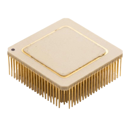
Common questions
Product FAQ
Targeted answers for buyers verifying the exact XC5VLX50T-1FFG665C ordering code, packaging, stock, datasheet, and replacement path.
What does XC5VLX50T-1FFG665C mean?
XC5VLX50T-1FFG665C is the exact ordering code listed for a Embedded - FPGAs (Field Programmable Gate Array) component from Xilinx. The current package reference is BGA, with listed context including IC FPGA 360 I/O 665FCBGA. Buyers should use the full code when requesting stock, price, datasheet, or compliance confirmation.
How should buyers verify the XC5VLX50T-1FFG665C ordering code?
Treat XC5VLX50T-1FFG665C as the full ordering code during RFQ and engineering review. Confirm the listed BGA package, manufacturer documentation from Xilinx, datasheet ordering table, reel or packing details, and any customer approval constraints before substitution or PO release.
What package is XC5VLX50T-1FFG665C supplied in?
XC5VLX50T-1FFG665C is currently listed with package reference BGA from Xilinx. Buyers should confirm the manufacturer package drawing, footprint, pinout, tape-and-reel details, and receiving requirements before approval.
Is XC5VLX50T-1FFG665C in stock at TrustCompo?
This page currently displays 1 public stock records for XC5VLX50T-1FFG665C with 157 listed pieces. Before ordering, confirm the package (BGA), required quantity, live availability, lead time, final price, date code, MOQ, packaging evidence, and RFQ documentation.
Where can I compare XC5VLX50T-1FFG665C alternatives?
A mapped alternative list is not currently published for XC5VLX50T-1FFG665C. Send an RFQ with the target quantity, package constraints, and approval requirements so TrustCompo can help review credible replacement options.