

CD4097BPW Interface - Analog Switches, Multiplexers, Demultiplexers by Texas Instruments
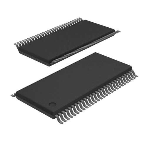
CD4097BPW is a Interface - Analog Switches, Multiplexers, Demultiplexers from Texas Instruments in TSSOP packaging. It is commonly reviewed for IC MUX/DEMUX DUAL 1X8 24TSSOP. This page lists current TrustCompo stock, tier pricing, package data, datasheet access, compliance attributes, Hong Kong warehouse shipping options, payment confirmation, and RFQ options for buyers verifying this exact ordering code.
Pictures are for reference only. Please contact us for the latest pictures.

- 365-Day GuaranteeAfter-sales support helps buyers handle quality questions with a clearer return and review window.
- Ships within 24-48 HoursAvailable items can move quickly once the quote, quantity, and delivery details are confirmed.
- 100% Anti-Counterfeit TestedParts are checked through authenticity-focused handling and inspection before shipment.
Key specifications
- Part Number
CD4097BPW
- Internal code
TCE000041862
- Package
TSSOP
- Manufacturer
- Texas Instruments
Key specifications
- Series
-
- Min Quantity
1
- Category
- Integrated Circuits (ICs)
- Description
IC MUX/DEMUX DUAL 1X8 24TSSOP
- key Attributes
-
Trust signals
Quality and trust signals
Review TrustCompo quality credentials, traceability support, anti-counterfeit handling, and inspection controls before sending an RFQ.
4 certifications
ISO 9001
Quality management processes for more consistent sourcing and handling.
AS9120B
Aerospace-focused distribution controls for traceability and reliability.
ISO 14001
Environmental management discipline across warehouse and operating workflows.
ESD Control
Electrostatic handling standards to help protect sensitive components.
RFQ checklist
Order process
Confirm the core buying details for CD4097BPW before RFQ, PO release, and shipment planning.
- 1
Confirm MPN
Use the exact part number, manufacturer, package, and approval constraints in the RFQ.
- 2
Check stock and price
Verify live availability, MOQ, lead time, final unit price, and tax terms before PO release.
- 3
Align documents
Confirm datasheet, CoC, traceability, lifecycle notes, and inspection scope when required.
- 4
Arrange shipment
Release the PO and align DHL, FedEx, UPS, or buyer forwarder shipment from Hong Kong.
Before PO release
Part confirmation
- Exact MPN confirmed: CD4097BPW
- Package to verify: TSSOP
Commercial confirmation
- Live stock and lead time confirmed by RFQ
- Final price and tax terms confirmed before PO release
Fulfillment & documents
- Ship-from location: Hong Kong warehouse
- Shipping method: DHL, FedEx, UPS, or buyer forwarder account
Product overview
Product overview
Review the sourcing context for CD4097BPW from Texas Instruments, including product identity, application fit, package notes, and purchasing considerations.
Description CD4067BMS and CD4097BMS CMOS analog multiplexers/demultiplexers
* are digitally controlled analog switches having low ON Impedance, low OFF leakage current, and internal address decoding. In addition, the ON resistance is relatively constant over the full input-signal range.
Features
• High Voltage Types (20V Rating)
• CD4067BMS Single 16 Channel Multiplexer/Demultiplexer
• CD4097BMS Differential 8 Channel Multiplexer/Demultiplexer
• Low ON Resistance: 125Ω(typ) Over 15Vp-p Signal Input Range for VDD - VSS = 15V
• High OFF Resistance: Channel Leakage of ±10pA (typ) at VDD - VSS = 18V
• Matched Switch Characteristics: RON = 5Ω(typ) for VDD - VSS = 15V
• Very Low Quiescent Power Dissipation Under All Digital Control Input and Supply Conditions: 0.2µW (typ) at VDD - VSS = 10V
• Binary Address Decoding on Chip
• 5V, 10V and 15V Parametric Ratings
• 100% Tested for Quiescent Current at 20V
• Maximum Input Current of 1µA at 18V Over Full Package Temperature Range; 100nA at 18V and +25oC
• Standardized Symmetrical Output Characteristics Applications
• Analog and Digital Multiplexing and Demultiplexing
• A/D and D/A Conversion
• Signal Gating
* When these devices are used as demultiplexers the “CHANNEL IN/OUT” terminals are the outputs and the “COMMON OUT/IN” terminals are the inputs.
Technical parameters
Parameters
Compare grouped CD4097BPW parameters from Texas Instruments, including package, series, key attributes, and technical values used for engineering and sourcing review.
Product Attribute
Packaging
Tube
Product Attribute
Length
7.8mm
Product Attribute
Package / Case
24-TSSOP (0.173, 4.40mm Width)
Product Attribute
Pin Count
24
Product Attribute
Thickness
1mm
Product Attribute
Width
4.4mm
| Parameter | Value |
|---|---|
Packaging Indicates the form of delivery for the component, such as tape and reel, tube, or tray. This affects handling, storage, and assembly processes. Verify the packaging type matches your production requirements and equipment compatibility. | Tube |
Length Specifies the physical length of the component body, typically in millimeters. This dimension is critical for PCB layout and mechanical fit. Verify against the datasheet to ensure proper clearance and alignment in your design. | 7.8mm |
Package / Case Physical package or case type of the component, defining its dimensions, mounting style, and thermal characteristics. Common types include SMD, through-hole, BGA, and QFN. Choose the package that fits your PCB layout and assembly process. Verify the exact package code in the datasheet for footprint compatibility. | 24-TSSOP (0.173, 4.40mm Width) |
Pin Count Total number of pins or terminals on the component package. Essential for footprint design, PCB layout, and connector mating. Verify against the datasheet to ensure compatibility with your board and assembly process. | 24 |
Thickness Thickness of the component, a critical dimension for PCB clearance, enclosure fit, and thermal performance. This measurement is especially important for capacitors, inductors, and connectors. Ensure the thickness meets your design constraints and does not interfere with adjacent components. Check the datasheet for tolerance and recommended mounting height. | 1mm |
Width Physical width of the component body, typically in millimeters. Essential for PCB footprint design and mechanical fit. Verify against the datasheet to ensure proper clearance and compatibility with your board layout and enclosure. | 4.4mm |
Height Physical height of the component, measured from the mounting surface to the topmost point. This dimension is critical for clearance in compact assemblies and for ensuring proper fit within enclosures. Always verify against the datasheet for tolerance and mounting considerations. | 1.2mm |
Weight Specifies the physical weight of the electronic component, important for logistics, shipping cost, and mechanical design. Verify the exact weight in the datasheet or packaging information, as it may vary with packaging type and quantity. | 89.499445mg |
Terminal Pitch Terminal pitch is the center-to-center distance between adjacent leads or pads on a component. It determines PCB layout compatibility and soldering feasibility. Verify against the datasheet to ensure your footprint matches the component's actual lead spacing. | 0.65mm |
Contact Plating Specifies the metal coating applied to the contact surfaces of connectors, switches, or relays. This finish affects conductivity, corrosion resistance, and durability. Engineers should verify the plating material and thickness against the datasheet to ensure reliable performance in the intended environment. | Gold |
Lead Free Indicates whether the component is manufactured without lead, complying with RoHS and similar regulations. Check this attribute to ensure environmental compliance for your market. Verify against the datasheet for exact material declarations. | Lead Free |
Pb-Free Code Indicates whether the component is lead-free per RoHS or other directives. Buyers use this to verify environmental compliance and avoid restricted substances. Always confirm with the datasheet or certificate of compliance. | yes |
REACH Status Shows whether the component complies with the EU REACH regulation. Essential for legal market access in Europe. Check the manufacturer's latest statement to confirm that no substances of very high concern are present above the threshold. | REACH Unaffected |
ECCN Export Control Classification Number assigned by the U.S. government. Determines whether the component requires an export license. Essential for international trade compliance. Verify the ECCN with the manufacturer or supplier before shipping to avoid legal issues. | EAR99 |
Manufacturer'S Part No. The unique part number assigned by the original component manufacturer. Use this to cross-reference datasheets, verify specifications, and ensure the exact component matches your design requirements. Always confirm the number against the manufacturer's official documentation. | CD4097BPW |
Categories Lists the product categories or classifications assigned to this component, such as connectors, capacitors, or modules. This helps in filtering and comparing similar parts. Review the categories to ensure the component fits your application and to find alternative parts in the same class. | Integrated Circuits (ICs) |
Technology Manufacturing technology or process used for the component, such as thin film, thick film, or semiconductor process. Affects performance, stability, and cost. Confirm the technology matches your application requirements and environmental conditions. | CMOS |
Sub-Categories Indicates the specific product subcategories or classifications within the broader component family. Helps narrow down search results and identify the exact type of component needed for your design. Review the subcategory to ensure compatibility with your application. | Interface - Analog Switches, Multiplexers, Demultiplexers |
Subcategory A more specific classification within the main product category, such as 'Ceramic Capacitor' under 'Capacitors'. This helps narrow down search results and compare similar components. Use it to filter products with similar characteristics and intended applications. | Multiplexer or Switches |
Base Part Number Identifies the core product family without package, grade, or option suffixes. Use this to compare equivalent components across manufacturers and to locate the primary datasheet. Verify the full ordering code against the manufacturer's specification before design-in. | CD4097 |
Lifecycle Status Current stage in the product's lifecycle, such as Active, Obsolete, or End of Life. This indicates availability and long-term supply risk. Check this before designing in a part to ensure it will be available for your product's production lifetime. | ACTIVE (Last Updated: 3 days ago) |
Factory Lead Time Indicates the typical duration from order confirmation to shipment from the manufacturer's facility. This helps you plan production schedules and inventory. Verify current lead times with your distributor or supplier, as they may vary based on order quantity, product availability, and market conditions. | 6 Weeks |
Part Status Lifecycle status of the part, such as active or obsolete. Indicates availability and long-term support from the manufacturer. Check this before design-in to avoid last-time buys or supply disruptions. Verify with the datasheet or distributor for current status. | Active |
Manufacturer Identifies the company that designed and produced the component. Buyers often filter by manufacturer to ensure brand reliability, quality standards, and supply chain consistency. Verify the manufacturer against the datasheet and official packaging to avoid counterfeit parts. | Texas |
Number Of Functions Specifies the count of independent functions or channels integrated into a single component package. This helps engineers determine if the part can handle multiple signal paths or operations simultaneously. Verify against the datasheet to ensure the device meets your circuit's functional requirements. | 1 |
Number Of Terminations Indicates the total number of electrical connection points on the component, such as pins or pads. This is critical for PCB footprint design and assembly. Verify it matches the package specification to ensure proper soldering and connectivity. | 24 |
Number Of Bits Bit width of digital data processed by a converter, processor, or memory. Higher bits mean better resolution or precision. Verify against datasheet to match your system's data width and accuracy needs. | 8 |
Voltage - Supply, Single (V+) Specifies the single positive supply voltage required for the component's operation. This is a key parameter for power design and compatibility. Always verify the absolute maximum ratings and recommended operating range in the datasheet to avoid damage and ensure stable performance. | 3V~18V |
Radiation Hardening Indicates if the component is designed to withstand ionizing radiation in space, nuclear, or high-energy physics applications. Compare radiation-tolerant vs. radiation-hardened parts for mission-critical designs. Verify the total ionizing dose (TID) and single-event effect (SEE) ratings in the datasheet. | No |
Bandwidth Indicates the frequency range over which the component operates effectively. Compare bandwidth when selecting amplifiers, filters, or data converters. Verify the specified bandwidth against your signal frequency requirements and the datasheet's test conditions to ensure optimal performance. | 20MHz |
Operating Supply Current The amount of current the device draws from its power supply during normal operation. This is essential for power budget calculations, thermal management, and selecting appropriate power sources. Check datasheet for typical and maximum values under specified conditions. | 80nA |
Resistance Electrical resistance value in ohms, defining opposition to current flow. Critical for current limiting, voltage division, and signal conditioning. Always check tolerance and power rating in the datasheet for reliable circuit operation. | 240Ohm |
Max Power Dissipation Maximum power the component can safely dissipate as heat without damage. Exceeding this may cause failure. Check datasheet for thermal resistance and derating curves under your operating conditions. | 500mW |
Terminal Form Describes the physical configuration of the component's leads or pads, such as through-hole, surface mount, or gull-wing. This affects PCB layout, soldering process, and mechanical fit. Confirm compatibility with your assembly method and footprint. | GULL WING |
Supply Voltage Specifies the nominal operating voltage that must be applied to the component for proper function. Verify this value against your system's power rail and the datasheet's absolute maximum ratings to ensure reliable operation and avoid damage. | 5V |
Mounting Type Specifies how the component attaches to the PCB or assembly, such as surface mount, through-hole, or chassis mount. This affects soldering process, mechanical stability, and thermal performance. Verify compatibility with your board layout and assembly capabilities. | Surface Mount |
Operating Temperature Specifies the ambient temperature range within which the component reliably functions. Compare this with your application's thermal environment to ensure proper operation. Always verify against the datasheet for derating curves and maximum ratings. | -55°C~125°C TA |
Number Of Pins Total number of pins or contacts on the component. This determines the footprint and mating connector requirements. Always match the pin count to your PCB layout and connector specification to ensure proper electrical and mechanical connection. | 24 |
Peak Reflow Temperature (Cel) Maximum temperature during reflow soldering that the component can withstand. This is critical for solder joint reliability and preventing damage. Verify that the peak reflow temperature is compatible with your soldering profile and the component's moisture sensitivity level. | 260 |
Minimum Supply Voltage Specifies the lowest DC input voltage at which the component reliably operates. Compare this value with your system's power rail tolerances and the device's recommended operating conditions to ensure stable performance across all load and temperature ranges. | 3V |
Nominal Supply Current Typical current drawn from the supply under nominal operating conditions. Compare this value across similar components to estimate power consumption and thermal behavior. Always verify against the datasheet for your specific voltage and load conditions. | 100μA |
Mounting Type Specifies how the component is attached to the PCB, such as through-hole or surface mount. This affects assembly processes, thermal performance, and mechanical strength. Buyers should verify compatibility with their manufacturing capabilities and design requirements. | Surface Mount |
Terminal Position Position of the terminals on the package, such as dual-in-line, gull-wing, or J-lead. This affects PCB layout, soldering, and thermal performance. Engineers must ensure the terminal position matches the footprint and assembly capabilities of their manufacturing line. | DUAL |
Number Of Circuits Specifies the total number of independent electrical paths or circuits within the component. This is critical for connectors, switches, and relay arrays to match the required wiring scheme. Always verify against the datasheet to ensure the circuit count meets your application's needs. | 2 |
Max Supply Voltage Indicates the highest DC or AC voltage that can be safely applied to the power supply pin without risking damage or malfunction. Verify this limit against the datasheet before designing your circuit to ensure reliable operation under all conditions. | 18V |
| Parameter | Value |
|---|---|
HTSUS Harmonized Tariff Schedule of the United States code for customs classification. Essential for import/export documentation and duty calculation. Verify the correct code with a trade specialist to avoid customs delays. | 8542.39.0001 |
REACH SVHC Indicates whether the product contains substances of very high concern as per the REACH regulation. Buyers should verify this for compliance with EU environmental standards, especially when exporting to Europe. Check the manufacturer's declaration or datasheet for accurate SVHC status. | No SVHC |
Moisture Sensitivity Level (MSL) Indicates the floor life of a component before it must be baked prior to soldering. Higher levels require stricter handling and shorter exposure times. Verify the MSL rating in the datasheet to ensure proper storage and assembly conditions. | 1 (Unlimited) |
RoHS Status Indicates whether the component complies with the EU RoHS directive restricting hazardous substances. Buyers should verify this status for regulatory compliance and market access. Check the datasheet or certificate for exact compliance details. | ROHS3 Compliant |
JESD-609 Code This code indicates the terminal finish material per JESD-609 standard. It helps identify the plating type for soldering compatibility and environmental compliance. Check the datasheet for the exact code and its meaning. | e4 |
| Parameter | Value |
|---|---|
Maximum Supply Current Indicates the highest current the device draws from its power supply under specified conditions. Compare this value when evaluating power budgets and thermal management. Always verify against the datasheet for your operating voltage and load. | 0.6mA |
Current - Leakage (IS(Off)) (Max) Maximum leakage current flowing through the switch when it is in the off state. This parameter affects power consumption and signal integrity in high-impedance circuits. Compare values to ensure the device meets your system's standby or off-state requirements, and verify against the datasheet for operating conditions. | 100nA |
Supply Type Indicates the required power source, such as AC or DC, for the component. Engineers compare this to ensure compatibility with the system's power architecture. Verify the supply type against the datasheet to avoid incorrect power connections. | Single |
On-State Resistance Match-Nom Indicates the nominal matching of on-state resistance between multiple channels in a device, such as a dual MOSFET or analog switch. This parameter is critical for parallel operation and current sharing. Verify the specified match against the datasheet to ensure balanced performance. | 15Ohm |
Logic Function Specifies the Boolean operation performed by the logic IC, such as AND, OR, NAND, or XOR. Engineers compare this to match the required signal processing in their circuit. Verify the exact function against the datasheet to ensure correct logic behavior. | Demultiplexer, Multiplexer |
Turn-Off Delay Time Measures the time from when the turn-off command is applied to when the device actually begins to switch off. This delay affects switching losses and timing in power circuits. Engineers compare this parameter to ensure proper synchronization and to minimize power dissipation during high-frequency operation. | 440 ns |
Power Supplies Specifies the required power supply voltages for the component. Engineers use this to ensure the board's power rails match the device's needs. Verify against the datasheet's recommended operating conditions to avoid undervoltage or overvoltage issues. | 5/15V |
Mux/Demux Circuit Configuration Defines the switch topology, such as 2:1, 4:1, or 8:1, indicating how many inputs are routed to outputs. Essential for selecting the correct multiplexer for signal routing in your design. Check the datasheet for channel count and switching characteristics. | 8:1 |
Propagation Delay Specifies the time interval between an input transition and the corresponding output transition. Critical for timing analysis in digital circuits. Verify against datasheet for specific test conditions, supply voltage, and load capacitance. | 60 ns |
Channel-To-Channel Matching (ΔRon) Indicates the maximum difference in on-resistance between any two channels in a multi-channel switch or multiplexer. This parameter affects signal integrity and accuracy in analog routing applications. Compare this value when selecting devices for precision measurement or audio systems. | 5 Ω |
Analog IC - Other Type Select this category when the analog integrated circuit does not fit standard classifications like op-amps, comparators, or regulators. Verify the exact function and pinout in the datasheet to ensure compatibility with your circuit design and performance requirements. | DIFFERENTIAL MULTIPLEXER |
Number Of Channels Specifies how many independent signal paths or outputs the component provides. Compare this value with your circuit requirements to ensure each channel can be used separately. Verify the channel configuration in the datasheet, as some devices may share pins or have internal connections. | 2 |
Turn On Delay Time Time from when the input signal crosses its threshold until the output begins to turn on. This parameter affects switching speed and power dissipation in high-frequency circuits. Verify it against the datasheet for your specific load and drive conditions. | 650 ns |
Channel Capacitance (CS(Off), CD(Off)) Capacitance between source and drain terminals when the switch is off. This parasitic capacitance affects high-frequency performance, switching speed, and signal integrity. Lower values are preferred for RF and high-speed digital applications. Verify against datasheet for voltage and frequency conditions. | 0.2pF 35pF |
On-State Resistance (Max) Maximum resistance between the switch terminals when the device is fully on. Lower values reduce power loss and heat. Compare this parameter when selecting MOSFETs, IGBTs, or relays for high-current circuits. Always verify against the datasheet for your operating conditions. | 240Ohm |
Notice documents
PCN / product notice documents
0 documents
No public PCN / PDN records currently displayed
No public product notice document is currently displayed for CD4097BPW. Confirm PCN, PDN, EOL, date code, and lifecycle status during RFQ before production purchase.
Related sourcing options
Recommended products
Explore related Interface - Analog Switches, Multiplexers, Demultiplexers products to compare fit, stock status, datasheets, and sourcing options.


Common questions
Product FAQ
Targeted answers for buyers verifying the exact CD4097BPW ordering code, packaging, stock, datasheet, and replacement path.
What does CD4097BPW mean?
CD4097BPW is the exact ordering code listed for a Interface - Analog Switches, Multiplexers, Demultiplexers component from Texas Instruments. The current package reference is TSSOP, with listed context including IC MUX/DEMUX DUAL 1X8 24TSSOP. Buyers should use the full code when requesting stock, price, datasheet, or compliance confirmation.
How should buyers verify the CD4097BPW ordering code?
Treat CD4097BPW as the full ordering code during RFQ and engineering review. Confirm the listed TSSOP package, manufacturer documentation from Texas Instruments, datasheet ordering table, reel or packing details, and any customer approval constraints before substitution or PO release.
What package is CD4097BPW supplied in?
CD4097BPW is currently listed with package reference TSSOP from Texas Instruments. Buyers should confirm the manufacturer package drawing, footprint, pinout, tape-and-reel details, and receiving requirements before approval.
Is CD4097BPW currently available?
CD4097BPW is currently marked with stock availability on this page. Before ordering, confirm the package (TSSOP), listed stock (80966), available quantity (12863), required quantity, lead time, final price, compliance needs, and exact ordering code match through RFQ.
Where can I compare CD4097BPW alternatives?
A mapped alternative list is not currently published for CD4097BPW. Send an RFQ with the target quantity, package constraints, and approval requirements so TrustCompo can help review credible replacement options.